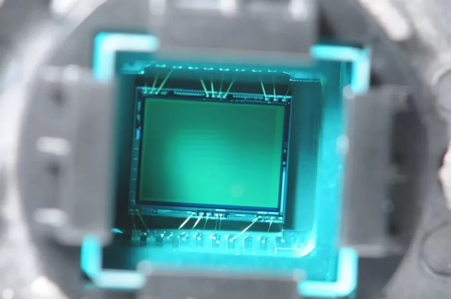
Sony’s next-generation image sensor will be based on a multi-layer structure. The image sensor is composed of five layers: the silicon substrate, an organic light-emitting diode (OLED) layer, a photodiode, an electromagnetic wave-guiding layer, and a reflective layer. This technology will contribute to the development of next-generation digital imaging products.
The technology also promises to offer improved low-temperature performance as well as improved durability for applications in harsh environments such as on the surface of satellites or in space.
The conventional method
Sony has been working on its own image sensor technology named Sony IMX250, which is a 2D/3D multi-layered image sensor. It’s a high-performance, low-power CMOS sensor made with a dual-layer structure.
The aim of its development is to achieve high sensitivity and low power consumption in the camera.
The new technology
The big news is that Sony is working on a new imaging technology named “Multi-Layer Imager” (MLI). The technology has the potential to revolutionize camera design and improve the performance of today’s digital cameras.
The basic principle behind MLI is that it combines two existing technologies: an advanced CMOS sensor and an advanced CMOS image signal processor. The combined technology uses an advanced digital signal processor to convert the raw RAW digital data into the signal processed by this CMOS sensor. The data obtained from a number of sensors can be processed in parallel for optimum processing efficiency, even when different lenses are used for one image or when different data are recorded during recording.
The technology has been introduced as part of the “Sony A7 III” camera and will also appear in “Sony A6500” and “Sony Alpha 7 II” cameras at some point next year.
Advantages of the new method
Sony is working on a new technology that will allow them to put two or more layers of transistors and photodiodes together, thereby providing significant advantages.
The company is calling it “multi-layered”, but the idea is to make it possible to stack several components, with different functions running at the same time. There are no known limitations to how high the number of layers can go.
A Sony engineer involved in the project told Reuters: “In conventional in-house image sensors, we have a single transistor and photodiode combination. But with this technology, you have a silicon wafer with several transistors and photodiodes stacked on top of each other.”
Sony has said that this technology promises to solve problems caused by power losses and heat generated during image processing. It can also lower manufacturing costs by reducing wiring density.
Conclusion
Sony is working on a multi-layer image sensor for smartphones and I think people will start seeing this new technology in 2022 smartphones.
You must be logged in to post a comment.